Operational amplifier

An operational amplifier, often called an 'op-amp', is a DC-coupled high-gain electronic voltage amplifier with differential inputs and, usually, a single output. Typically the output of the op-amp is controlled either by negative feedback, which largely determines the magnitude of its output voltage gain, or by positive feedback, which facilitates regenerative gain and oscillation. High input impedance at the input terminals and low output impedance are typical characteristics.
Op-amps are among the most widely used electronic devices, used in a vast array of consumer, industrial, and scientific devices. Many standard IC op-amps cost only a few cents in moderate production volume; however some integrated or hybrid operational amplifiers with special performance specifications may cost over $100 US in small quantities.
Modern designs are electronically more rugged than earlier implementations and some can sustain direct short-circuits on their outputs without damage.
Contents |
[edit] History
An op-amp, defined as a general-purpose, DC-coupled, high gain, inverting feedback amplifier, is first found in US Patent 2,401,779 "Summing Amplifier" filed by Karl D. Swartzel Jr. of Bell labs in 1941. This design used three vacuum tubes to achieve a gain of 90dB and operated on voltage rails of ±350V. In contrast to modern day op-amps, it had a single inverting input and an output instead of the modern two differential inputs where one is inverting and the other is not. Throughout WWII, Swartzel's design proved its value by being liberally used in the M9 artillery director designed at Bell Labs. This artillery director worked with the SCR584 radar system to achieve extraordinary hit rates (near 90%) that would not have been possible otherwise.
In 1947, the op-amp was first formally defined and named in a paper by Professor John R. Ragazzoni. In this same paper a footnote mentioned an op-amp design by a student that would turn out to be quite significant. This op-amp, designed by Loebe Julie, was superior in a variety of ways. It had two major innovations. Its input stage used a long-tailed triode pair with loads matched to reduce drift in the output and, far more importantly, it was the first op-amp design to have two inputs (both inverting and non-inverting). The differential input made a whole range of new functionality possible, but it would not be used for a long time due to the rise of the chopper-stabilized amplifier.
In 1949, Edwin A. Goldberg, designed a chopper stabilized op-amp. This set-up uses a normal op-amp with an additional AC amplifier that goes alongside the op-amp. The chopper gets an AC signal from DC by switching between the DC voltage and ground at a fast rate (60Hz or 400Hz). This signal is then amplified, rectified, filtered and fed into the op-amp's non-inverting input. This improved the gain of the op-amp while significantly reducing the output drift and DC offset. Unfortunately, any design that used a chopper couldn't use their non-inverting input for any other purpose. Nevertheless, the improved characteristics of the chopper-stabilized op-amp made it the dominant way to use op-amps. Techniques that used the non-inverting input regularly would not be very popular until the 1960s when op-amp ICs started to show up in the field.
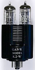
In 1953, vacuum tube op-amps became commercially available with the release of the K2-W from GAP/R. It sold in an octal package and had a (K2-P) chopper add-on available that would effectively "use up" the non-inverting input. This op-amp was based on a descendant of Loebe Julie's 1947 design and, along with its successors, would start the widespread use of op-amps in industry.
With the birth of the transistor in 1947, and the silicon transistor in 1954, the concept of ICs became a reality. The introduction of the planar process in 1959 made transistors and ICs stable enough to be commercially useful. By 1961, solid-state, discrete op-amps were being produced. These op-amps were effectively small circuit boards with packages such as edge-connectors. They usually had hand-selected resistors in order to improve things such as voltage offset and drift. The P45 (1961) had a gain of 94dB and ran on ±15V rails. It was intended to deal with signals in the range of ±10V. By 1962, several companies were producing modular potted packages that could be plugged into printed circuit boards. These packages were crucially important as they made the operational amplifier into a single black box which could be easily treated as a component in a larger circuit.
In 1963, the first monolithic IC op-amp, the μA702 designed by Bob Widlar at Fairchild Semiconductor, was released. Monolithic ICs consist of a single chip as opposed to a chip and discrete parts (a discrete IC) or multiple chips bonded and connected on a circuit board (a hybrid IC). Almost all modern op-amps are monolithic ICs; however, this first IC did not meet with much success. Issues such as an uneven supply voltage, low gain and a small dynamic range held off the dominance of monolithic op-amps until 1965 when the μA709[1] (also designed by Bob Widlar) was released. The popularity of monolithic op-amps was further improved upon the release of the LM101 in 1967, which solved a variety of issues and the subsequent release of the μA741 in 1968. The μA741 was extremely similar to the LM101 except that Fairchild's facilities allowed them to include a 30pF compensation capacitor inside the chip instead of requiring external compensation. This simple difference has made the 741 the canonical op-amp and many modern amps base their pinout on the 741's.The μA741 is still in production, and has become ubiquitous in electronics — many manufacturers produce a version of this classic chip, recognizable by part numbers containing "741."
Since the 741, there have been many different directions taken in op-amp design. Varactor bridge op-amps started to be produced in the late 1960s; they were designed to have extremely small input current are still amongst the best op-amps available in terms of common-mode rejection with the ability to correctly deal with 100s of Volts at its inputs. In the 1970s high speed, low-input current designs started to be made by using FETs. These would be largely replaced by op-amps made with MOSFETs in the 1980s. During the 1970s single sided supply op-amps also became available. The LM324 (released in 1972) was one such op-amp that came in a quad package and became an industry standard. In addition to packaging multiple op-amps in a single package, the 1970s also saw the birth of op-amps in hybrid packages. These op-amps were generally improved versions of existing monolithic op-amps and were without a doubt the best op-amps available. As the properties of monolithic op-amps improved, the more complex hybrid ICs were quickly relegated to systems that are required to have extremely long service lives or other specialty systems.
[edit] Timeline
1941: First (vacuum tube) op-amp
1947: First op-amp with an explicit non-inverting input
1948: First chopper-stabilized op-amp9
1961: First discrete IC op-amps
1962: First op-amps in potted modules
1963: First monolithic IC op-amp
1966: First varactor bridge op-amps
1968: Release of the μA741 - would be seen as a nearly ubiquitous chip
1970: First high-speed, low-input current FET design
1972: Single sided supply op-amps being produced
[edit] Circuit notation

The circuit symbol for an op-amp is shown in Figure 1
where:
- V+: non-inverting input
- V−: inverting input
- Vout: output
- VS+: positive power supply
- VS−: negative power supply
The power supply pins (VS+ and VS−) can be labeled in different ways (See IC power supply pins). Despite different labeling, the function remains the same. Often these pins are left out of the diagram for clarity, and the power configuration is described or assumed from the circuit. The positions of the inverting and non-inverting inputs may be reversed in diagrams where appropriate; the power supply pins are not commonly reversed. For Example IC741 is an operational amplifier. It is used for doing arithmetic operations on analog computers, instrumentation and other control systems. Operational amplifier is in the class of linear IC's. Linear have a peculiarity that they can take continuous voltage signals like their analog counterparts.These are highly used today because of their high reliability and low cost. They are mainly used as voltage amplifiers. The basic operational amplifier works similar to the following sequence.
input stage--->intermediate stage--->level shifter--->output stage.
Input stage consists of high input impedance it amplifies the difference between the given input signals. The intermediate stage consists of cascaded amplifiers to amplify the signals from the input. Due to high amplification the DC level of the signals goes up. So in order to bring them down to the rated value,level shifter or level translator is used. The output stage consists of class AB/ class B power amplifier in order to amplify the power of the output signal.
[edit] Operation of ideal op-amps
The amplifier's differential inputs consist of an inverting input and a non-inverting input, and ideally the op-amp amplifies only the difference in voltage between the two. This is called the "differential input voltage". In its most common use, the op-amp's output voltage is controlled by feeding a fraction of the output signal back to the inverting input. This is known as negative feedback. If that fraction is zero, i.e., there is no negative feedback, the amplifier is said to be running "open loop" and its output is the differential input voltage multiplied by the total gain of the amplifier, as shown by the following equation:

where V+ is the voltage at the non-inverting terminal, V− is the voltage at the inverting terminal and G is the total open-loop gain of the amplifier.
Because the magnitude of the open-loop gain is typically very large and not well controlled by the manufacturing process, op-amps are not usually used without negative feedback. Unless the differential input voltage is extremely small, open-loop operation results in op-amp saturation (see below in Nonlinear imperfections). An example of how the output voltage is calculated when negative feedback exists is shown below in Basic non-inverting amplifier circuit.
Another typical configuration of op-amps is the positive feedback, which takes a fraction of the output signal back to the non-inverting input. An important application of it is the comparator with hysteresis (see Schmitt trigger).
For any input voltages the ideal op-amp has
- infinite open-loop gain,
- infinite bandwidth,
- infinite input impedances (resulting in zero input currents),
- zero offset voltage,
- infinite slew rate,
- zero output impedance, and
- zero noise.
The inputs of an ideal op-amp under negative feedback can be modeled using a nullator, the output with a norator and the combination (complete ideal op-amp) by a nullor.
[edit] Limitations of real op-amps
Real op-amps can only approach this ideal: in addition to the practical limitations on slew rate, bandwidth, offset and so forth mentioned above, real op-amp parameters are subject to drift over time and with changes in temperature, input conditions, etc. Modern integrated FET or MOSFET op-amps approximate more closely the ideal op-amp than bipolar ICs where large signals must be handled at room temperature over a limited bandwidth; input impedance, in particular, is much higher, although the bipolar op-amps usually exhibit superior (i.e., lower) input offset drift and noise characteristics.
Where the limitations of real devices can be ignored, an op-amp can be viewed as a black box with gain; circuit function and parameters are determined by feedback, usually negative. IC op-amps as implemented in practice are moderately complex integrated circuits; see the internal circuitry for the relatively simple 741 op-amp below, for example.
[edit] DC imperfections
Open-loop gain is defined as the amplification from input to output without any feedback applied. For most practical calculations, the open-loop gain is assumed to be infinite; in reality it is obviously not. Typical devices exhibit open-loop DC gain ranging from 100,000 to over 1 million; this is sufficiently large for circuit gain to be determined almost entirely by the amount of negative feedback used. Op-amps have performance limits that the designer must keep in mind and sometimes work around. In particular, instability is possible in a DC amplifier if AC aspects are neglected.
Other imperfections include:
- Finite gain — the effect is most pronounced when the overall design attempts to achieve gain close to the inherent gain of the op-amp.
- Finite input resistance — this puts an upper bound on the resistances in the feedback circuit. Some op-amps have circuitry to protect inputs from excessive voltage: this makes input parameters slightly worse. Some op-amps are available in protected (thus slightly degraded) and unprotected versions.
- Nonzero output resistance — important for low resistance loads. Except for very small voltage output, power considerations usually come into play first. (Output impedance is inversely proportional to the idle current in the output stage — very low idle current results in very high output impedance.)
- Input bias current — a small amount of current (typically ~10 nA for bipolar op-amps, or picoamperes for CMOS designs) flows into the inputs. This current is mismatched slightly between the inverting and non-inverting inputs (there is an input offset current). This effect is usually important only for very low power circuits.
- Input offset voltage — the voltage required across the op-amp's input terminals to drive the output voltage to zero.[2] In the perfect amplifier, there would be no input offset voltage. However, it exists in actual op-amps because of imperfections in the differential amplifier that constitutes the input stage of the vast majority of these devices. Input offset voltage creates two problems: First, due to the amplifier's high voltage gain, it virtually assures that the amplifier output will go into saturation if it is operated without negative feedback, even when the input terminals are wired together. Second, in a closed loop, negative feedback configuration, the input offset voltage is amplified along with the signal and this may pose a problem if high precision DC amplification is required or if the input signal is very small.[3]
- Common mode gain — A perfect operational amplifier amplifies only the voltage difference between its two inputs, completely rejecting all voltages that are common to both. However, the differential input stage of an operational amplifier is never perfect, leading to the amplification of these identical voltages to some degree. The standard measure of this defect is called the common-mode rejection ratio (denoted, CMRR). Minimization of common mode gain is usually important in non-inverting amplifiers (described below) that operate at high amplification.
- Temperature effects — all parameters change with temperature. Temperature drift of the input offset voltage is especially important.
[edit] AC imperfections
The op-amp gain calculated at DC does not apply at higher frequencies. To a first approximation, the gain of a typical op-amp is inversely proportional to frequency. This means that an op-amp is characterized by its gain-bandwidth product. For example, an op-amp with a gain bandwidth product of 1 MHz would have a gain of 5 at 200 kHz, and a gain of 1 at 1 MHz. This low-pass characteristic is introduced deliberately, because it tends to stabilize the circuit by introducing a dominant pole. This is known as frequency compensation.
Typical low cost, general purpose op-amps exhibit a gain bandwidth product of a few megahertz. Specialty and high speed op-amps can achieve gain bandwidth products of hundreds of megahertz. For very high-frequency circuits, a completely different form of op-amp called the current-feedback operational amplifier is often used.
Other imperfections include:
- Finite bandwidth — all amplifiers have a finite bandwidth. This creates several problems for op amps. First, associated with the bandwidth limitation is a phase difference between the input signal and the amplifier output that can lead to oscillation in some feedback circuits. The internal frequency compensation used in some op amps to increase the gain or phase margin intentionally reduces the bandwidth even further to maintain output stability when using a wide variety of feedback networks. Second, reduced bandwidth results in lower amounts of feedback at higher frequencies, producing higher distortion, noise, and output impedance and also reduced output phase linearity as the frequency increases.
- Input capacitance — most important for high frequency operation because it further reduces the open loop bandwidth of the amplifier.
- Common mode gain — See DC imperfections, above.
[edit] Nonlinear imperfections
- Saturation — output voltage is limited to a minimum and maximum value close to the power supply voltages.[4] Saturation occurs when the output of the amplifier reaches this value and is usually due to:
- In the case of an op-amp using a bipolar power supply, a voltage gain that produces an output that is more positive or more negative than that maximum or minimum; or
- In the case of an op-amp using a single supply voltage, either a voltage gain that produces an output that is more positive than that maximum, or a signal so close to ground that the amplifier's gain is not sufficient to raise it above the lower threshold.[5]
- Slewing — the amplifier's output voltage reaches its maximum rate of change. Measured as the slew rate, it is usually specified in volts per microsecond. When slewing occurs, further increases in the input signal have no effect on the rate of change of the output. Slewing is usually caused by internal capacitances in the amplifier, especially those used to implement its frequency compensation.
- Non-linear transfer function — The output voltage may not be accurately proportional to the difference between the input voltages. It is commonly called distortion when the input signal is a waveform. This effect will be very small in a practical circuit if substantial negative feedback is used.
[edit] Distortion in op-amps
Very often operational amplifiers are used for audio filters. It is important the evaluation of the distortion introduced by the Distortion Multiplication Factor (Kd) described by Oscar Bonello [6] The behavior of this type of operational amplifiers is important to get low distortion amplifiers and audio consoles for sound recording and reproduction.
[edit] Power considerations
- Limited output current — the output current must obviously be finite. In practice, most op-amps are designed to limit the output current so as not to exceed a specified level — around 25 mA for a type 741 IC op-amp — thus protecting the op-amp and associated circuitry from damage.
- Limited dissipated power — an opamp is a linear amplifier. It therefore dissipates some power as heat, proportional to the output current, and to the difference between the output voltage and the supply voltage. If the opamp dissipates too much power, then its temperature will increase above some safe limit. The opamp may enter thermal shutdown, or it may be destroyed.
[edit] Applications
[edit] Use in electronics system design
The use of op-amps as circuit blocks is much easier and clearer than specifying all their individual circuit elements (transistors, resistors, etc.), whether the amplifiers used are integrated or discrete. In the first approximation op-amps can be used as if they were ideal differential gain blocks; at a later stage limits can be placed on the acceptable range of parameters for each op-amp.
Circuit design follows the same lines for all electronic circuits. A specification is drawn up governing what the circuit is required to do, with allowable limits. For example, the gain may be required to be 100 times, with a tolerance of 5% but drift of less than 1% in a specified temperature range; the input impedance not less than 1 megohm; etc.
A basic circuit is designed, often with the help of circuit modeling (on a computer). Specific commercially available op-amps and other components are then chosen that meet the design criteria within the specified tolerances at acceptable cost. If not all criteria can be met, the specification may need to be modified.
A prototype is then built and tested; changes to meet or improve the specification, alter functionality, or reduce the cost, may be made.
[edit] Basic non-inverting amplifier circuit
The general op-amp has two inputs and one output. The output voltage is a multiple of the difference between the two inputs (some are made with floating, differential outputs):
- Vout = G(V+ − V−)
G is the open-loop gain of the op-amp. The inputs are assumed to have very high impedance; negligible current will flow into or out of the inputs. Op-amp outputs have very low source impedance.
If the output is connected to the inverting input, after being scaled by a voltage divider K = R1 / (R1 + R2), then:

- V+ = Vin
- V− = K Vout
- Vout = G(Vin − K Vout)
Solving for Vout / Vin, we see that the result is a linear amplifier with gain:
- Vout/Vin = G /(1 + G K)'
If G is very large, Vout/Vin comes close to 1/K, which equals 1 + (R2/R1).
This negative feedback connection is the most typical use of an op-amp, but many different configurations are possible, making it one of the most versatile of all electronic building blocks.
When connected in a negative feedback configuration, the op-amp will try to make Vout whatever voltage is necessary to make the input voltages as nearly equal as possible. This, and the high input impedance, are sometimes called the two "golden rules" of op-amp design (for circuits that use negative feedback):
- No current will flow into the inputs.
- The input voltages will be nearly equal.
The exception is if the voltage required is greater than the op-amp's supply, in which case the output signal stops near the power supply rails, VS+ or VS−.
Most single, dual and quad op-amps available have a standardized pin-out which permits one type to be substituted for another without wiring changes. A specific op-amp may be chosen for its open loop gain, bandwidth, noise performance, input impedance, power consumption, or a compromise between any of these factors.
[edit] Other applications
- audio- and video-frequency pre-amplifiers and buffers
- voltage comparators
- differential amplifiers
- differentiators and integrators
- filters
- precision rectifiers
- precision peak detectors
- voltage and current regulators
- analog calculators
- analog-to-digital converters
- digital-to-analog converter
- voltage clamps
- oscillators and waveform generators
- ↑ A.P. Malvino, Electronic Principles (2nd Ed.1979. ISBN 0-07-039867-4) p.476.
- ↑ D.F. Stout Handbook of Operational Amplifier Circuit Design (McGraw-Hill, 1976, ISBN 007061797X ) p. 1-11. This definition hews to the convention of measuring op-amp parameters with respect to the zero voltage point in the circuit, which is usually half the total voltage between the amplifier's positive and negative power rails.
- ↑ Many older designs of operational amplifiers have offset null inputs to allow the offset to be manually adjusted away. Modern precision op-amps can have internal circuits that automatically cancel this offset using choppers or other circuits that measure the offset voltage periodically and subtract it from the input voltage.
- ↑ That the output cannot reach the power supply voltages is usually the result of limitations of the amplifier's output stage transistors. See "Output stage," below.
- ↑ The output of older op-amps can reach to within one or two volts of the supply rails. The output of newer so-called "rail to rail" op-amps can reach to within millivolts of the supply rails when providing low output currents.
- ↑ “Distortion in Positive- and Negative-Feedback Filters”, Oscar Bonello. Journal of Audio Engineering Society, New York, Vol 32 # 4, April 1984
| |
Some content on this page may previously have appeared on Citizendium. |